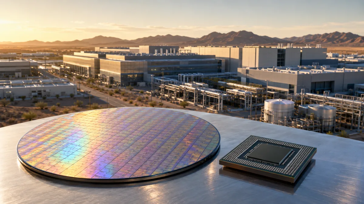
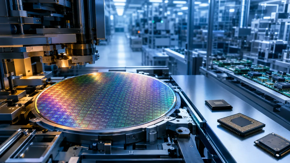
India has approved a fresh ₹1.28 lakh crore expansion of its semiconductor programme, moving its chip strategy from a first wave of headline projects towards the more difficult work of building an industrial ecosystem.
The immediate number is substantial. But the more important question is what the money will buy. A semiconductor industry is not created by announcing fabrication plants alone. It requires reliable power and water, specialised chemicals and gases, equipment maintenance, design talent, packaging capacity, patient capital and customers willing to qualify locally produced chips.
That makes the new phase less about proving political intent and more about proving execution.
What India has approved
The government has allocated an additional ₹1.28 lakh crore for its semiconductor programme, according to a July 15 announcement reported by Reuters. The fresh support extends India’s effort to reduce its dependence on imported chips and capture a larger share of the global electronics value chain.
The expansion builds on the first semiconductor incentive programme and on projects already approved in Gujarat and Assam. Those include a wafer fabrication plant planned by Tata Electronics with Taiwan’s Powerchip Semiconductor Manufacturing Corporation, as well as assembly, testing, marking and packaging facilities involving Tata, Micron, CG Power and other partners.
The distinction matters. Wafer fabrication is the most technically and financially demanding part of the chain, while assembly and testing can help India build manufacturing knowledge, supplier networks and export capacity sooner. A resilient strategy needs both.
Why the second phase matters more than the first
India has already demonstrated that it can assemble smartphones and other electronics at scale. Semiconductors are a different challenge. Production tolerances are microscopic, equipment is extraordinarily expensive and a small process failure can destroy the economics of an entire line.
The next programme therefore needs to close gaps around the factory, not simply subsidise more factories. Domestic suppliers of specialty chemicals, substrates, gases, components and precision services will determine how much value remains in India. Without them, a plant may manufacture chips locally while remaining heavily dependent on imported inputs.
This is also why packaging deserves attention. Advanced packaging is becoming strategically important as chipmakers combine multiple specialised dies or chiplets into a single system. India can use its existing strength in engineering and electronics manufacturing to compete in this layer while its fabrication capabilities mature.
The AI boom changes the opportunity
Global demand is being reshaped by artificial intelligence. Data centres require advanced processors, high-bandwidth memory, networking silicon and power-management chips. At the same time, cars, industrial equipment, telecom networks and consumer devices continue to need large volumes of mature-node semiconductors.
India does not need to begin by chasing only the smallest process nodes used in flagship AI accelerators. Mature and specialised chips can serve automotive, defence, energy, telecom and industrial customers, where dependable supply and long product cycles matter as much as transistor density.
A portfolio approach would reduce the risk of treating semiconductor leadership as a single prestige project. Design incentives, compound semiconductors, sensors, power electronics, packaging and manufacturing equipment can each create defensible capabilities.
Talent will be the limiting infrastructure
Capital can purchase tools and construct clean rooms. It cannot instantly produce experienced process engineers, equipment technicians, yield specialists and manufacturing managers.
India has a large semiconductor design workforce, but fabrication requires a different mix of skills. The most effective training will need to connect universities and technical institutes directly with operating plants. Apprenticeships, vendor-led certification and international industry partnerships will be more useful than classroom capacity alone.
The country will also need to retain experienced professionals. Global chip expansion means engineers are in demand across the United States, Taiwan, Japan, South Korea and Europe. India’s projects must offer credible career paths, not only construction-phase employment.
What success should look like
The programme should ultimately be judged by production and competitiveness rather than sanctioned investment. Useful measures would include operational capacity, manufacturing yield, domestic value addition, export revenue, supplier localisation and the number of Indian-designed chips reaching commercial volume.
Timelines also require realism. Semiconductor plants take years to build, qualify and ramp. Early delays do not automatically mean failure, but repeated changes in technology, partners or commercial assumptions should receive close scrutiny.
India’s advantage is that it combines a large domestic electronics market, engineering talent, policy support and companies seeking alternatives in a concentrated global supply chain. Its disadvantage is that incumbents have decades of accumulated process knowledge and dense supplier clusters.
The ₹1.28 lakh crore expansion gives India another chance to narrow that gap. The money is an important input. Whether it produces a durable chip industry will depend on the less visible work that begins after the announcement.